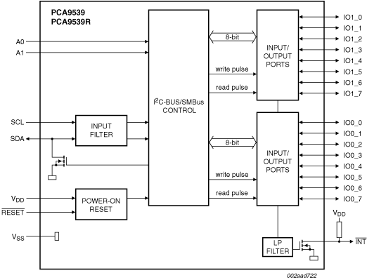
The PCA9539; PCA9539R is a 24-pin CMOS device that provides 16 bits of General Purpose parallel Input/Output (GPIO) expansion with interrupt and reset for I2C-bus/SMBus applications and was developed to enhance the NXP Semiconductors family of I2C-bus I/O expanders. I/O expanders provide a simple solution when additional I/O is needed for ACPI power switches, sensors, push buttons, LEDs, fans, etc.
The PCA9539; PCA9539R consists of two 8-bit configuration (input or output selection), input, output and polarity inversion (active HIGH or active LOW operation) registers. The system controller can enable the I/Os as either inputs or outputs by writing to the I/O configuration bits. The data for each input or output is kept in the corresponding Input or Output register. The polarity of the read register can be inverted with the Polarity inversion register. All registers can be read by the system controller.
The PCA9539; PCA9539R is identical to the PCA9555 except for the removal of the internal I/O pull-up resistor which greatly reduces power consumption when the I/Os are held LOW, replacement of A2 with RESET and a different address range.
The PCA9539; PCA9539R open-drain interrupt output is activated when any input state differs from its corresponding input port register state and is used to indicate to the system controller that an input state has changed.
The power-on reset sets the registers to their default values and initializes the device state machine. In the PCA9539, the RESET pin causes the same reset/default I/O input configuration to occur without de-powering the device, holding the registers and I2C-bus state machine in their default state until the RESET input is once again HIGH. This input requires a pull-up to VDD. In the PCA9539R however, only the device state machine is initialized by the RESET pin and the internal general-purpose registers remain unchanged. Using the PCA9539R RESET pin will only reset the I2C-bus interface should it be stuck LOW to regain access to the I2C-bus. This allows the I/O pins to retain their last configured state so that they can keep any lines in their previously defined state and not cause system errors while the I2C-bus is being restored.
Two hardware pins (A0, A1) vary the fixed I2C-bus address and allow up to four devices to share the same I2C-bus/SMBus.