デザイン・ファイル
1 設計・ファイル
-
シミュレーションとモデル
NX3DV42GU IBIS model
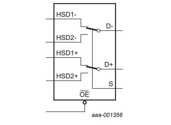
The NX3DV42 is a double-pole double-throw analog switch suitable for use as an analog or digital multiplexer/demultiplexer. Its wide bandwidth and low bit-to-bit skew allows the NX3DV42 to pass high-speed differential signals with good signal integrity. Its high channel to channel crosstalk rejection results in minimal noise interference. The bandwidth is wide enough to pass high-speed USB 2.0 differential signals (480 Mb/s). It consist of two switches, each with two independent input/outputs (HSDn+ and HSDn-) and a common input/output (D+ or D-). One digital inputs (S) is used to select the switch position. When pin OE is HIGH, the switches are turned off. Schmitt trigger action at the select input (S) and enable input (OE) makes the circuit tolerant to slower input rise and fall times across the entire VCC range from 3.0 V to 4.3 V.
部品番号: NX3DV42GM, NX3DV42GU, NX3DV42GU10, NX3DV42GU33.
クイック・リファレンス ドキュメンテーションの種類.
1 設計・ファイル
NXPから直接サポートを受けるには、以下のサイトをご覧ください。 エンジニアリング・サービス.
2 エンジニアリング・サービス

本製品をサポートするパートナーの一覧は、 パートナーマーケットプレイス.